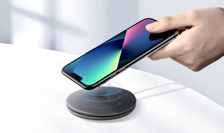
What is a gallium nitride (GaN) charger?
The GaN charger is a new type of power adapter made of GaN semiconductor material. Compared with traditional silicon-based (Si) chargers, GaN materials significantly improve the performance of power devices due to their physical properties, making the charger achieve breakthroughs in volume, efficiency, power density, etc., becoming the core carrier of fast charging technology.
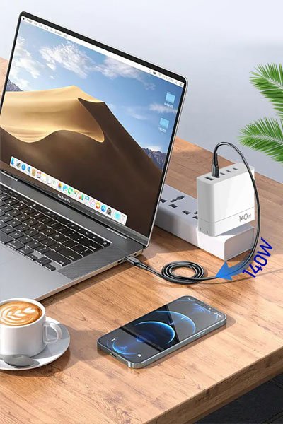
The core advantages of GaN chargers
- Smaller size and higher power density
Material properties: GaN’s electron mobility is about 5 times higher than silicon, and its breakdown field strength is 10 times that of silicon, allowing devices to operate at higher voltages and frequencies.
Structural optimization: GaN power devices (such as MOSFET) are more than 70% smaller than silicon-based devices, and the internal space utilization rate of the charger is higher. For example, the traditional 65W silicon-based charger is about the size of a mobile phone, while the GaN charger can be as small as a “cookie”.
- Higher efficiency and less heat generation
High frequency and low loss: GaN supports MHz-level high-frequency switching (traditional silicon-based is only at kHz level), which reduces the volume of transformers and capacitors while reducing switching losses, and the overall efficiency can reach more than 95%.
Temperature control advantage: Low loss means less heat accumulation. Combined with efficient heat dissipation design (such as boron nitride thermal conductive material), the temperature remains low even during long-term high-power operation.
- Support high-power fast charging, compatible with multiple devices
High power output: GaN charging heads can easily achieve power of more than 100W (such as laptop fast charging) and support fast charging protocols such as PD 3.1 and QC 4.0.
Multi-port intelligent allocation: A single charging head can power mobile phones, tablets, and laptops at the same time, and dynamically allocate power (such as three-port output: 100W+30W+18W).
- Safer and longer life
Resistant to high temperature and high pressure: GaN materials are much more stable than silicon at high temperatures, reducing the risk of short circuit or overheating.
Improved reliability: Reduced heat generation and component count, lower failure rates, and longer service life.

Comparison with traditional silicon-based chargers
| Feature | GaN Charger | Traditional Silicon-Based Charger |
| Size | 50%-70% smaller | Bulky, requires more heat dissipation |
| Max Power | Up to 240W (PD 3.1 EPR standard) | Typically below 100W |
| Efficiency | 92%-95% | 80%-85% |
| Heat Generation | Significantly reduced | Noticeable heating under high load |
| Cost | Higher (newer technology) | Lower (mature technology) |
Future trends of GaN chargers
Higher power: GaN is combined with silicon carbide (SiC) to develop towards 200W+ charging technology.
Wireless integration: GaN’s high-frequency characteristics help improve wireless fast charging efficiency.
Cost reduction: As technology becomes more popular, prices become more affordable and will gradually replace silicon-based chargers.
Gallium nitride chargers have redefined the balance between charging efficiency and volume through material innovation, becoming a benchmark in the era of fast charging. Their small size, high power, and low heat generation characteristics not only meet consumers’ demands for portability and speed, but also promote the development of electronic devices towards lightweight and high performance.
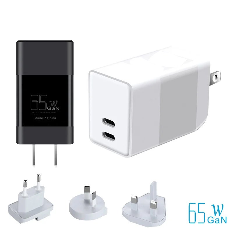
Safety issues and solutions for GaN chargers
Gallium nitride chargers are popular due to their high efficiency and small size, but their high power density and high-frequency operating characteristics also bring new safety challenges. The following are the main safety issues and corresponding solutions:
Core safety issues
- High temperature and thermal runaway risk
Problem: High-frequency switching and high-power output of GaN devices can cause localized high temperatures, leading to material aging, component failure, and even fire.
Risk scenarios: long-term full-load operation, insufficient heat dissipation design, and excessively high ambient temperature (such as use in a car in summer).
- High-frequency electromagnetic interference (EMI)
Problem: GaN devices can operate at frequencies up to the MHz level. High-frequency signals can easily generate electromagnetic radiation, interfering with other devices (such as mobile phones and wireless headphones) and even violating electromagnetic compatibility (EMC) standards.
Risk scenarios: When multiple devices are charging at the same time or near sensitive electronic devices.
- High voltage insulation failure
Problem: High-power charging heads need to support wide voltage input (such as 100-240V). If the insulating material (such as PCB substrate, packaging glue) has insufficient voltage resistance, it may cause leakage or breakdown.
Risk scenarios: voltage fluctuations, humid environment, and aging of insulation materials.
- Environmental protection and toxicity of materials
Problem: Some heat dissipation materials (such as lead-containing solder) or packaging materials may contain hazardous substances and do not comply with environmental regulations such as RoHS and REACH.
Risk scenario: Toxic substances are released when discarded charging heads are processed.
- Structural safety and short circuit risk
Problem: Miniaturized design results in small spacing between internal components, which can easily cause short circuits or arc discharges due to vibration and extrusion.
Risky scenarios: Bumps during transportation, loose internal components.
Solutions and Design Optimization
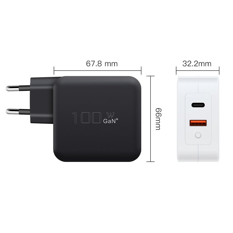
- Thermal management optimization
Solution: Use boron nitride (h-BN) and other high thermal conductivity insulation materials as the heat dissipation layer to improve the heat diffusion efficiency. Design a multi-layer heat dissipation structure (such as metal substrate + thermal conductive gel + heat dissipation fins). Add temperature sensors and over-temperature protection chips to automatically reduce power or cut off power when over-temperature occurs.
Verification standards: Passed IEC 62368-1 (thermal stress test) and UL 60950 (temperature rise test).
- Suppressing electromagnetic interference (EMI)
Solution: Add common-mode inductors, magnetic beads, and shielding covers to the circuit design to filter out high-frequency noise.
Optimize PCB layout, reduce high-frequency loop area, avoid cross-interference, and use soft switching technology (such as ZVS/ZCS) to reduce switching noise.
Verification standards: Complies with CISPR 32 (EMI emission limits) and FCC Part 15 Class B standards.
- High voltage insulation reinforcement
Solution: Use high CTI (Current Tracking Index) materials (such as PCB boards with FR-4 grade or above).
Use double insulation or reinforced insulation design in critical high voltage areas (such as primary-secondary isolation). Fill gaps with potting compounds (such as silicone) to enhance moisture resistance and insulation performance.
Verification standard: pass the withstand voltage test (such as 3000V AC/1 minute) and insulation resistance test (>100MΩ).
- Environmentally friendly material substitution
Solution: Ban the use of harmful substances such as lead and cadmium, and use halogen-free flame retardants (such as phosphorus-based flame retardants).
As heat dissipation materials, inorganic environmentally friendly materials such as boron nitride and aluminum oxide are preferred.
Verification standard: Passed RoHS 2.0, REACH SVHC testing.
- Structural safety design
Solution: Use mechanical fixation + glue reinforcement (such as epoxy resin) to prevent internal components from falling off due to vibration.
Optimize PCB layout to ensure that the distance between high-voltage and low-voltage lines meets safety requirements (such as creepage distance ≥ 4mm).
The shell is made of flame-retardant material (such as V-0 grade PC/ABS) and has passed the drop test (1m height, 6 sides 3 times).
Verification standards: Complies with IEC 60529 (foreign body intrusion protection) and UL 94 (flammability rating).
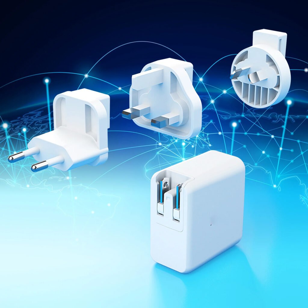
Certification and testing processes of GaN Chargers
To ensure safety, GaN chargers must pass the following international certifications:
Electrical safety: UL/EN/IEC 62368-1 (Safety standard for audio and video equipment).
EMC: FCC, CE (EN 55032/55035).
Energy efficiency: DoE Level VI, CoC Tier 2 (efficiency ≥ 90%).
Environmental protection: RoHS, REACH, WEEE.

